ECE1388 VLSI Design Methodology: Final Project
4 MHz DC-DC Converter with Low Power Current Sensor
Date of Submission: December 24, 2009
Members:
1. S M Ahsanuzzaman (Ahsan)
2. Seyed Behzad Mahdavikhah Mehrabad
3. Peng Zhao
Project Objective
The
objective of this project is to design and implement a fully integrated DC-DC
converter with low power current sensor. DC-DC converters are widely used to
supply power to all sorts of modern electronic devices; such as computers, LCD
monitors, cell phones, mp3 players, digital cameras etc. Fully integrated DC-DC
converters are very popular in low power portable electronic devices due to its
very high efficiency and small package size. A current sensor is often included
in the design for certain advantages such as: inherent current protection,
simplified control approach etc [1]. One of the major challenges of the current
sensor based approach is that it reduces the overall efficiency of the system
by introducing additional losses. In
this project a low power current sensor approach is taken to implement a fully
integrated DC-DC converter.
Design Overview and
Specifications
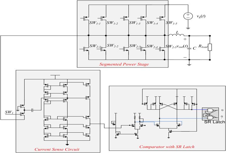
The block diagram of Fig. 1 shows
different modules of a DC-DC converter. Due to the big value of inductor and
capacitor (in the order of µ), these components would be off chip and the rest
of the converter would be on chip. In Fig. 1,
the blocks that are implemented in this project are marked with the rectangle
called ‘Integrated Chip’. This includes power MOSFETS (both NMOS and PMOS),
gate drivers, current sense circuit, comparator, SR latch, dead-time. The
controller is left for future development. In the close loop system the current
sensor extracts the information about the converter current (isense).
Similarly the controller senses the output voltage to generate the current
reference (iref).
These two currents are then compared using an analog comparator and the output
of the comparator resets the SR latch. The dead-time generator module generates
the gating signals for the power MOSFETS based on the output of the comparator.
Therefore, the chip will receive the source input voltage (3.3V), the sample of
the converter output voltage as the input voltage to the on chip digital
controller (named Vin in our chip) and a 1.5V input as
the operating voltage for our controller circuitry. Finally the output pin
(named Vx in our design) would be connected to the
off chip inductor.
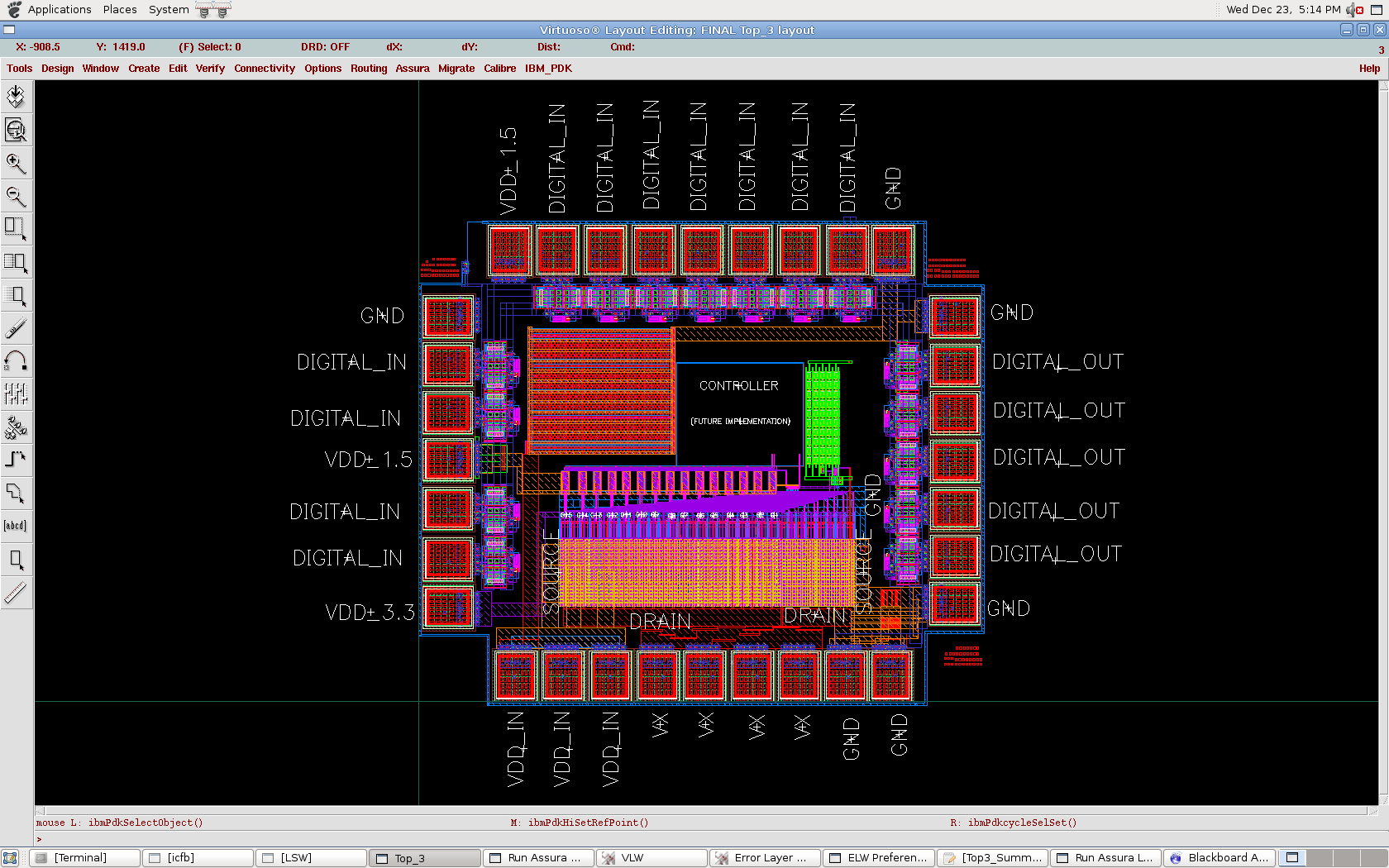
In
this project, the power mosfets, gate drivers and
input capacitor have been done by Ahsan,
Behzad did the Amplifier, dead time and pad design.
Current sensor and comparator are done by Peng.
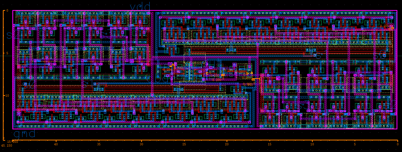
Fig. 2 depicts the full layout of our chip.
The following table summarizes the specification for our proposed
project:
|
Output Power |
400 mW |
|
Output Voltage |
1.2 V |
|
Input Voltage |
2.7 V – 3.3 V |
|
Switching Frequency |
4 MHz |
|
Process |
0.13 micron |
Table 1. Project Specifications
Block Design
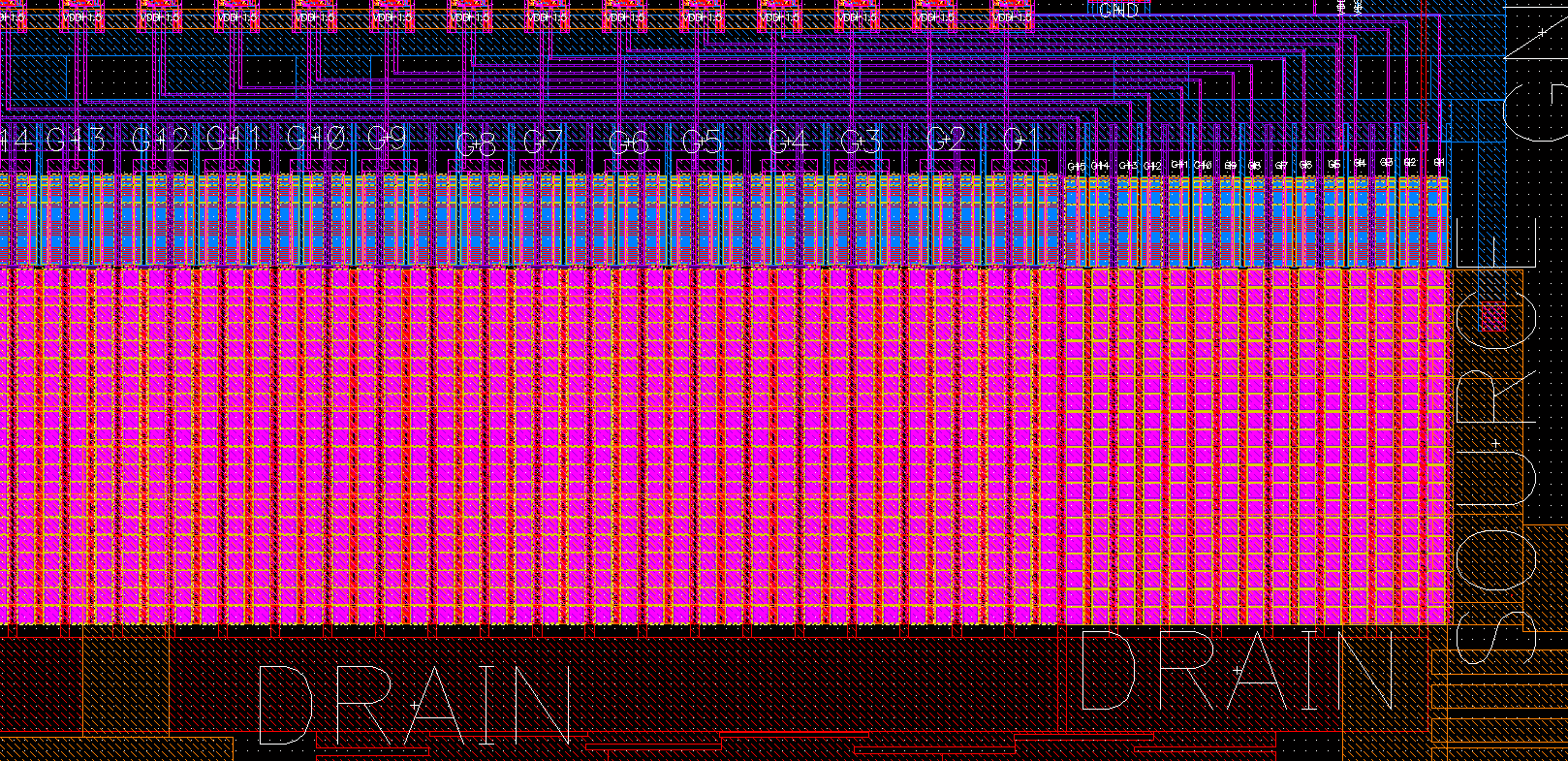
1. Power MOSFETs: Generally in a buck converter we need two
MOSFETs known as main switch and synchronous rectifier. These two MOSFETs work
in either triode or cut off region when the switch is on or off. To minimize Ron,
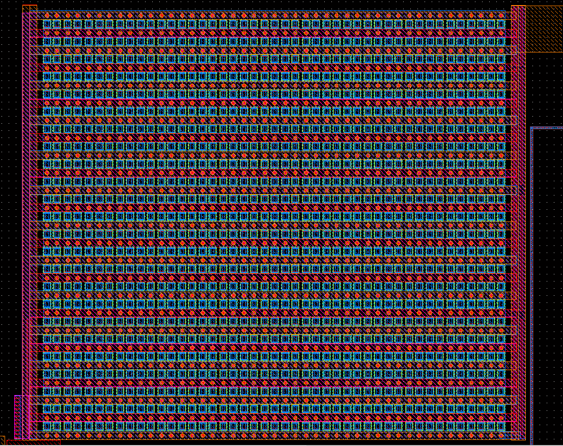
each of them is comprised by many MOSFETs, in our case 300 unit sized (w=60µ)
thick oxide NMOS for synchronous rectifiers and 900 PMOS for main switches. In
spite of loss reduction in switches during conduction the large number of
MOSFETs in parallel would have a large Cg, resulting in more
switching losses, which is more significant for small load currents. In our
design to compromise between conduction losses and switching losses, each of
the two switches is divided into 15 segments of parallel MOSFETs, therefore
depending on the load current; the controller determines how many of the
segments take part in current conduction. Fig.
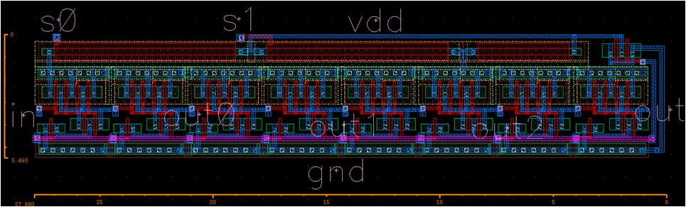
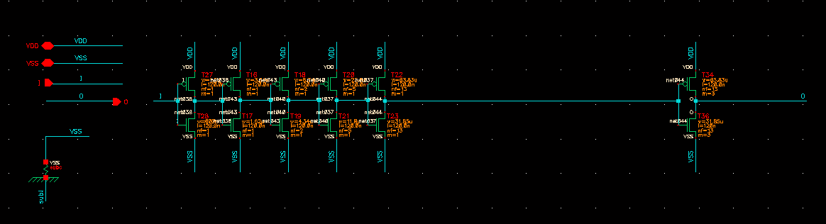
3 illustrates the layout of the power MOSFETs
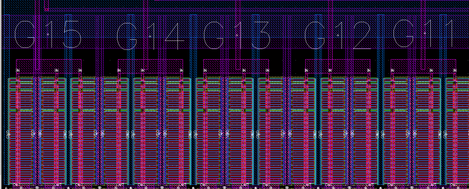
2. Gate Drivers: According to big value of Cg
of the switches, driving the MOSFETs directly with the output of the dead time
circuit introduces a delay associated with charging the gate capacitor. The gate driver block
consists of four inverters with appropriate sizing in series. Hence, it both
decouples the power switches from the dead time circuit and drives the gate of
the power switches with lower delay time. Fig.
4 illustrates the layout of the Gate drivers.
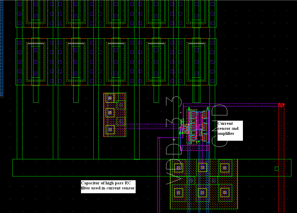
3. Current
Sensor: The current sensor is used to find the current
passing through the main power switches, the PMOS. To do this, we sense the
voltage drop across the PMOS, then by amplifying and inverting this value the
current is found. The current sensor in our design is composed of a sense-FET
and a high pass filter. The sense-FET is basically two transistors in series
which is in parallel with the PMOS. This sense-FET is followed by an RC high
pass filter. Therefore, the sense-FET brings a portion of the voltage drop across
the main switches to the high pass filter and the filter removes the DC value
of its input and passes it to the amplifier. Fig.
5 illustrates the layout of the Current sensor.
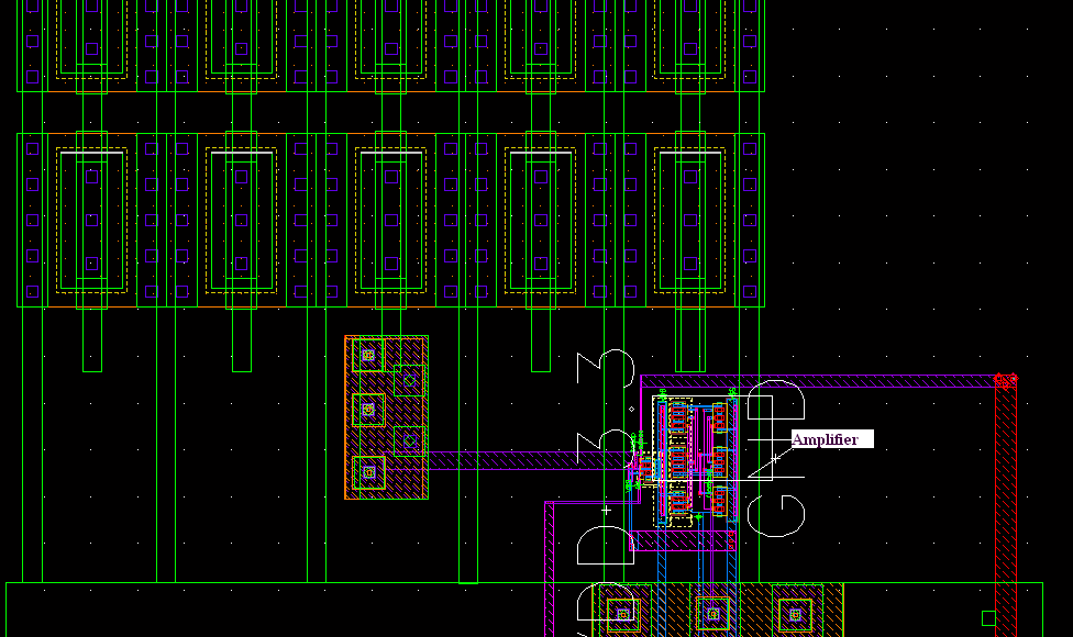
4.
Amplifier: A telescopic cascade amplifier is used to invert and
amplify the voltage drop across the main switches. This equals the current
passing through the PMOS multiplied by a gain. The schematic and layout of the
current sensor circuit are depicted in Fig. 6 and Fig. 7
5. Comparator: The comparator has two parts, a pre amplifier followed
by the comparator [2]. It performs the comparison between the output of the
current sensing circuitry and the reference current coming from the digital
controller. The schematic of the
comparator circuit is depicted in Fig. 6. Fig. 8 illustrates the layout of the comparator
followed by an SR latch.
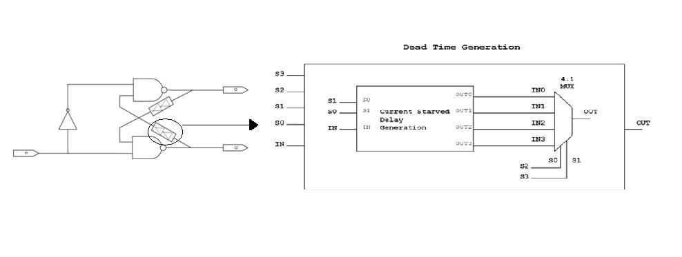
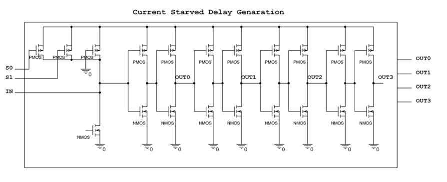
6. Dead Time
Generator: To
minimize losses during switching, a programmable dead time generator has been
used which is capable of generating 16 levels of delay between one and five nano seconds. This delay is generated using an SR latch
with programmable delay line generators in its feedback connection [3] as in Fig. 9.
The programmable delay generators consist of a current starved delay generation
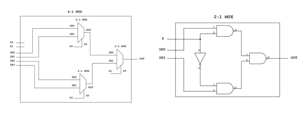
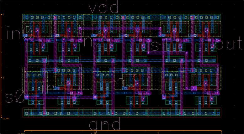
circuit followed by a 4:1 multiplexer, whose schematics are depicted in Fig. 10 and Fig. 11
respectively. Fig. 12, Fig. 13 and Fig. 14
illustrate the layout of the dead time generator, the 4:1 multiplexer and the
current starved delay generation circuit.
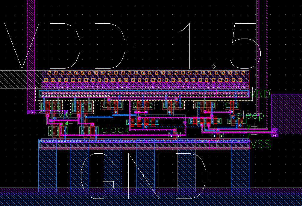
7. Input
Capacitor: A 100 fF
capacitor is placed between the ‘VDD’ and ‘GND’ inputs to eliminate the AC
noises on the input from the outside world. Fig.
15 illustrates the layout of the Input capacitor. This
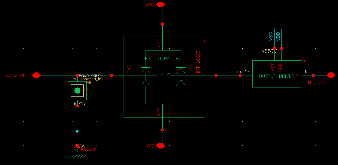
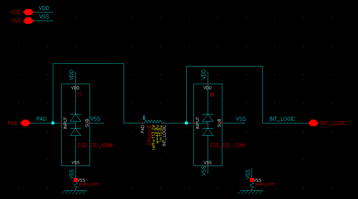
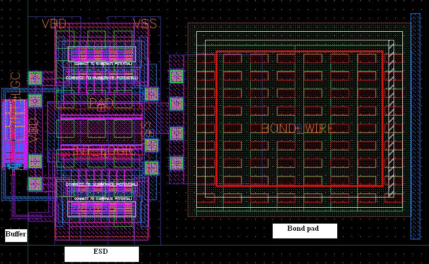
PAD Design: Two different types of pads have been used in our
design, one for analog inputs and outputs and the other for the digital inputs
and outputs. The difference is that the pads used for digital pins are
utilizing buffers. Moreover all these pads are protected from electrostatic
discharge (ESD). Fig. 16, Fig. 17 and Fig. 18 show the schematics of an input
digital pad, the ESD circuit and the input buffer. Fig. 19 illustrates the layout of a digital
buffered input pad, including the bond pad, ESD and buffer; the digital output
pads look similar. The analog input and output pads would look the same, but
excluding the buffer.
In the layout, a guard ring is utilized to
remove noise and the influence of different elements in the design, also the
digital and analog and power switch (relatively high frequency of high current
switching) circuitries have been shielded to isolate them from noises.
Appendix A (LVS Report): Follow the link: LVS Report
Appendix B (DRC Report): Follow the link: DRC Report
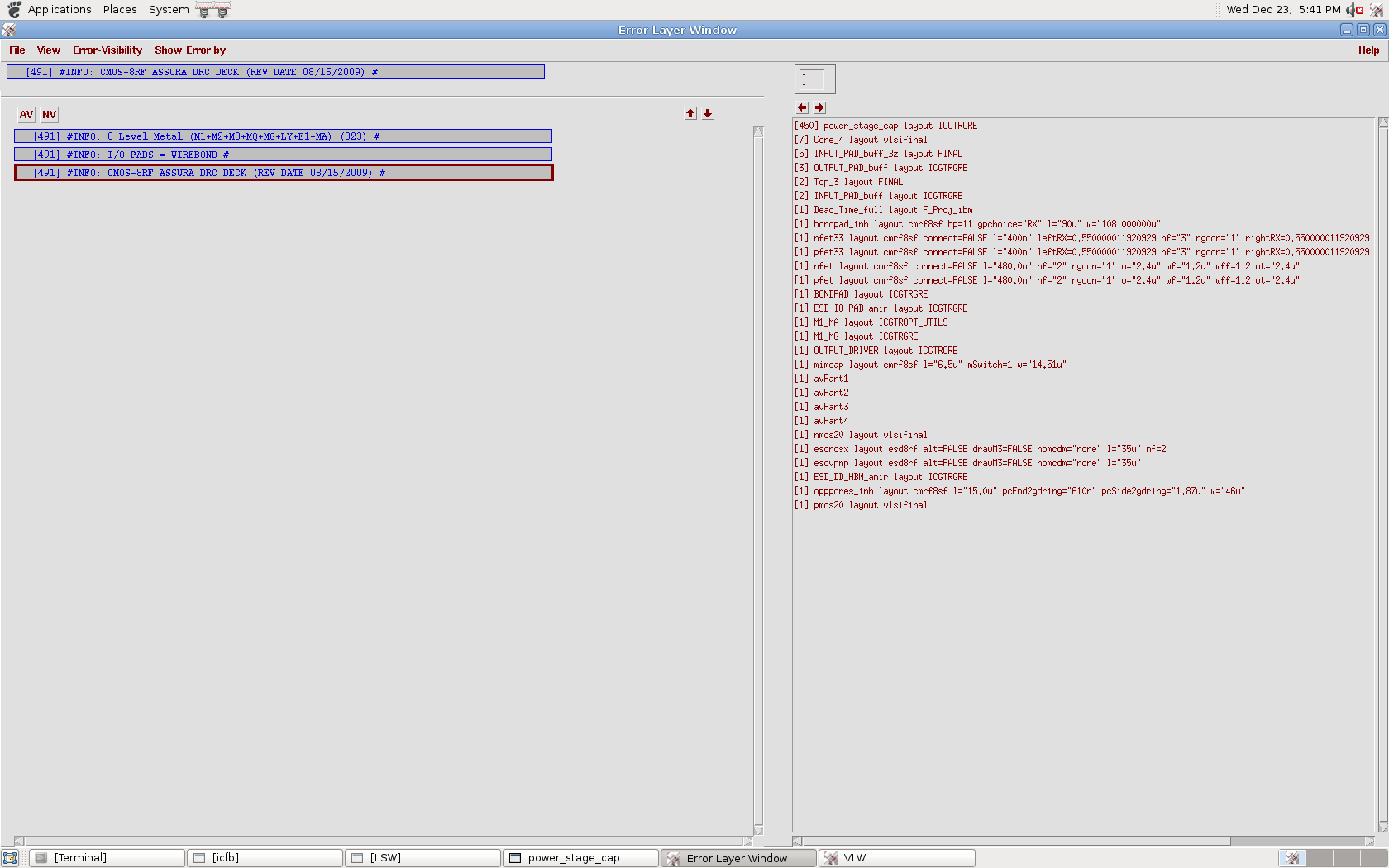
Moreover an screenshot of the error
free DRC Error layer window can be found here.
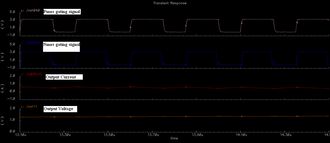
Appendix C (Simulation Result): Follow the
link: Top Level Simulation
References:
1-
Olivier Trescases, Integrated Power-Supplies
for Portable Applications, PhD thesis, Department of Electrical and Computer
Engineering, University of Toronto, 2007.
2-
Baker, R. J. 2002 Cmos: Mixed-Signal
Circuit Design. John Wiley & Sons, Inc.
3- Maymandi-Nejad, M. and Sachdev,
M. 2003. A digitally programmable delay element: design and analysis. IEEE Trans. Very
Large Scale Integr.
Syst. 11,
5 (Oct. 2003), 871-878. DOI= http://dx.doi.org/10.1109/TVLSI.2003.810787.