Research
Recent progress of nanofabrication technology has enabled researchers to achieve an unprecedented control of material properties. This advancement in fabrication technology has broadened the scope of photonics. It is now a key enabling technology for applications ranging from communications to life sciences, and holds great promises for future. My long term research goal is to transform the promises of photonics from possibility to reality. Within photonics my interest is broad: ranging from plasmonics, integrated optics and biosensing to gas sensing. Below is a short description of my key research areas.
Hybrid Plasmonic Waveguide
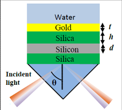
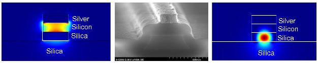
Surface plasmon (SP) is a surface wave which results from the coupling of an electromagnetic wave with the collective electronic oscillations at a metal-dielectric interface. SP has a number of unique features, and can be of great importance for practical applications. Unlike dielectric waveguides where light confinement is limited by diffraction, plasmonic waveguides can “squeeze” light to a subwavelength scale. This offers the possibility of scaling down photonic devices to the size of transistors which may result in successful integration of photonics and electronics. Since metal is part of a plasmonic waveguide, it suffers from a large propagation loss. This is a major limitation that has prevented plasmonics from becoming a more useful technology. I have proposed the hybrid plasmonic wavguide (HPWG) which can provide a better compromise between loss and confinement compared to many other previosuly reported plasmonic waveguides. It is compatible with silcon on insulator technology, and offers the possibilty of intergation of plasmonics and silicon photonics on the same platform. The work has been followed by many groups around the world. Many HPWG devices including nano-laser, couplers and sensors have been proposed and experimentally demonstarted. In addition to proposing the idea of HPWG, I have also work on the design and implementation of the HPWG waveguide devices for intergrated optics and biosensing. For example I have demonstrated the shortest broadband TE-pass polarizer on silicon on insulator platform. I also proposed a number of other devices including polarization rotator, broadbnad coupler and TM-pass polarizer.These devices are very compact and they can outperfrom existing designs in many respect.
Excitation of Surface Plasmon
Surface plasmon is usually excited by use of prism or grating. These excitation schemes are too bulky for nano-photonic applications. We have recently demonstrated that combination of a sub-wavelength slot and a dielectric waveguide can act as a very compact, low-noise and efficient plasmon excitation scheme.
Gain Assisted Surface Plasmon Propagation
The major limitation of surface plasmon is its large propagation loss. One possibility of overcoming this problem is to use an optical gain medium, e.g., quantum wells to compensate for this loss. I presented the first detailed theoretical analysis of the possibility of reduction of propagation loss of long range plasmon by using quantum wells as an optical gain medium. I showed that achieving lossless plasmon propagation is possible with existing technology - a prediction that was verified by several research group in last few years.

Hydrogen Sensor
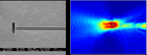
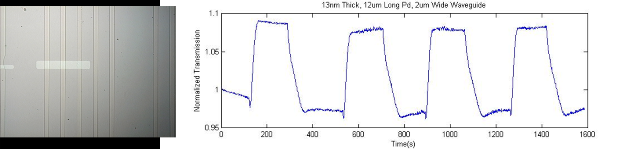
Hydrogen has numerous applications including oil refinery, semiconductor industry, aerospace and edible oil. With the current global energy crisis and increasing search for cleaner energy, hydrogen is also receiving more attention as an energy carrier. Being a very small molecule, hydrogen can easily leak through fissures and micro-cracks, and since the mixture of hydrogen and air is flammable and explosive for a wide range, such leaks pose very serious risk of accidents. There is an immediate need for a fast and reliable hydrogen sensor for safe storage, handling and use of hydrogen. I have experimentally demonstarted a compact integrated optic hydrogen sensor which consists of silicon waveguide coated with Palladium. IOur group is currently working on integrating this device with other sensors on the same chip to implemet an "Optical Nose". Such a sensor will be capable of simultaneous detection of multiple gases and less prone to give false alram with variation of temperature or humidity.
Biosensor
Optical sensing techinques are widely used for detection of various biomolecules. Plasmonis is one of the most popoular technique for optical biosensing. Since plasmonic sensors utilize only the transevrse magnetic (TM) polarization for measurement, the informaton obtained from such sensors is somewhat limited. For example iit is difficult to determine both adlayer thickness and index and one of them need to be known. Also it is difficult to differentiite between changes in bulk and surface properties using such sensors. The hybrid plasmonic guide that I proposed can support both trasnverse electric (TE) and transeverse magnetic (TM) polarization) it can obatin more information about biomolecules. In addition it is more senstivive than purely plasmonic sensor and provide an option of diffrentiating between change in bulk and surface index.