Current research
-
-
- Ultrafast injection of spin current in semiconductors
He studied generation of spin-polarized electrical currents by ultrafast optical excitation of semiconductors including GaAs, GaSb, and InP. Interband transition in these materials is induced by femtosecond laser pulses (~100 fs) of wavelength around 800 nm, and produces shift current and spin-polarized current depending on the beam polarization. Both types of currents produce terahertz (THz) radiation (wavelength ~100 micrometers) that can be detected using time-resolved electro-optic sampling.
- Analysis of laser beam interference for holographic fabrication of microstructures
Four laser beam interference can form various three-dimensional (3D) spatial intensity distribution with period on the order of laser wavelength. The periodic intensity distribution can be recorded in a photoresit to further fabricate 3D microstructures. He analyzed the relationship between the interfering Laser beams and the resulting spatial lattice and obtained multiple arrangements of four beams for the same type of any Bravais lattice. Those arrangements can compose a semi-continuous tunable lattice constant, which means in principle by using a single exposure wavelength one can fabricate lattices on a broad range of scale.
- Ultrafast injection of spin current in semiconductors
Let ‘light’ and ‘electron’ make ‘light devices’ on chip
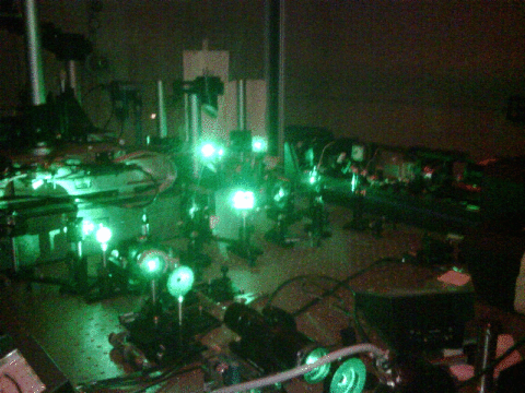
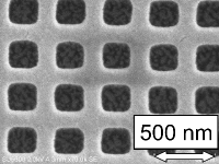
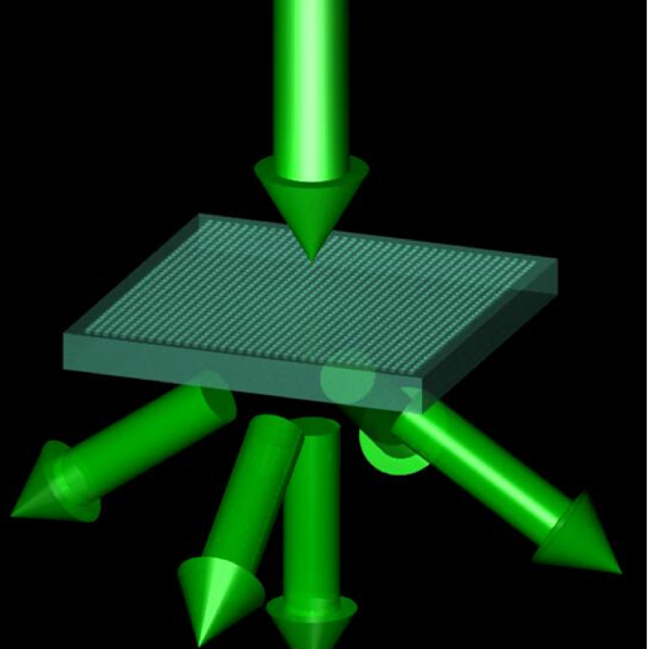
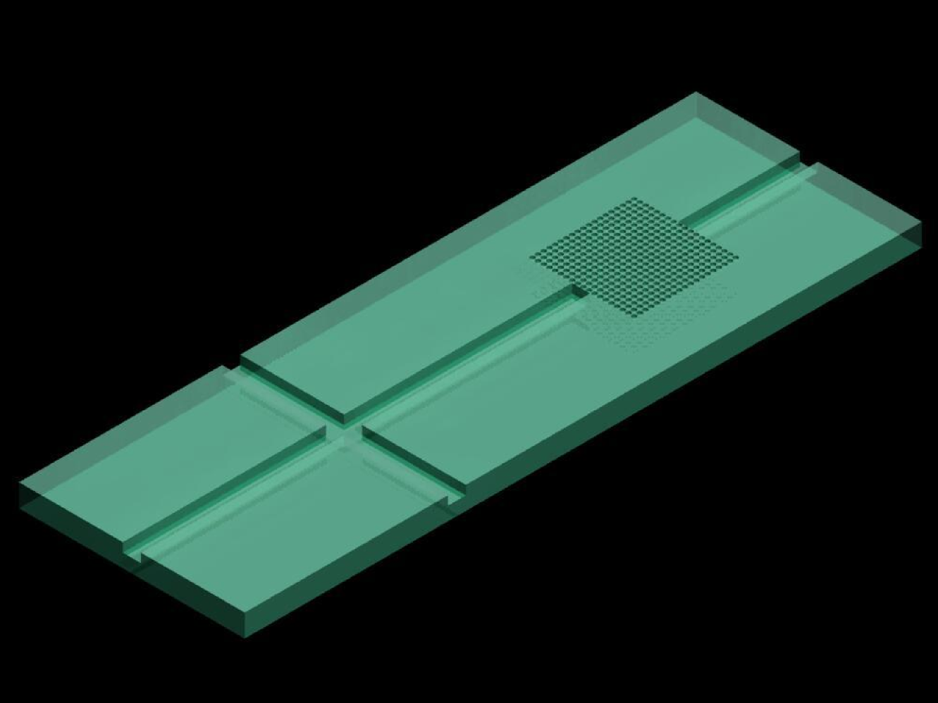
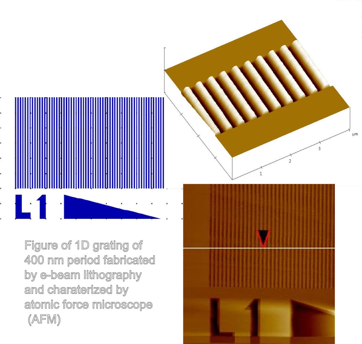
Leon uses electron beam lithography (EBL) to generate periodic nanoscale patterns (or grating structures) in resist, and then employs standard semiconductor cleanroom techniques, including spin coating, metal evaporation, lift-off, plasma dry etching and so on, to further process the nanostructures. In some cases, the grating structures in thin photoresist were fabricated by interference lithography. The above cartoon shows various facilities he works with.In another part of experiments, he fabricates submicron-gratings by EBL and takes the grating as a phase mask to expose thick photoresist against the mask using an Argon ion laser operating at 514.5 nm wavelength. He forms three-dimensional photonic crystal (PC) templates after development of the photoresist.
As a further step, he explores the cross-disciplinary applications of PC-embedded systems. More information of his research in three major parts is listed below:
Fabrication of diffractive phase masks by electron beam lithography and standard semiconductor cleanroom techniques
Ar+ laser exposure fabrication of 3D photonic crystal templates
Crossdisciplinary applications of photonic crystals
Previous research
Copyright 2015 Liang (Leon) Yuan, template shared by Rex Jones.