Project Title: Silicon texturization with low surface damage
Project Leader: Zahidur R Chowdhury
Supervisor: Prof. Nazir P. Kherani
Other Member(s): Zhou Lin [summer Student]
My role: Process optimization, train team members, characterization, report writing
Tools used: Oxford PlasmaLab 100 PECVD System / Sinton Silicon Lifetime Tester / Semilab’s µ-PCD lifetime tester / Mask aligner / Wet chemical processing / LATEX / Microsoft Office
Summary
- Low surface defect density of the textured crystalline silicon has been attained with appropriate wet chemical processing. The passivation quality was poor after the texturization steps resulting less than 10 μs minority carrier lifetime with hydrogen termination (in concentrated HF solution). The plasma damages were removed from the textured surfaces. An effective minority carrier lifetime more than 1.5 ms was obtained, measured using Sinton silicon lifetime testing tool. Textured silicon wafers were used to fabricated HIT cell with DC saddle field amorphous silicon and cell efficiency of 17% was achieved.
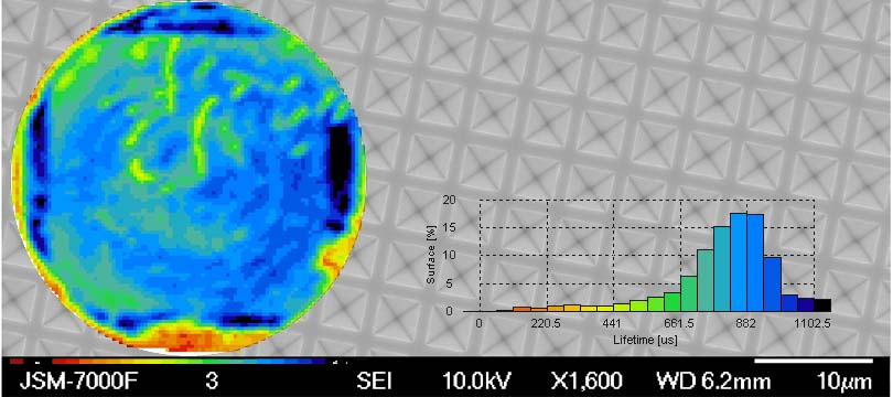
- Figure: (background) SEM image of the 5 μm inverted pyramid textured wafer (inset) spatial profile of the surface passivation quality of a 4-inch silicon wafer with textured front surface measured using μ-PCD tool.
Publication(s)
Zahidur R. Chowdhury and Nazir P. Kherani, “Facile grown oxide based passivation for silicon heterojunction PV cells”, presented in International Conference on Amorphous and Nanocyrstalline Semiconductor (ICANS), Toronto, Canada, 2013. view / link
[ Invited ] Nazir P. Kherani and Zahidur R. Chowdhury, “Facile native oxide based passivation of silicon: an unconventional approach”, presented in Materials Science & Technology 2013, Montreal, 2013. view / link
[ Invited ] Nazir P. Kherani and Zahidur R. Chowdhury, “Nanometer thick native oxide based passivation of silicon for high efficiency photovoltaics”, presented in International Nanoelectronics Conference (INEC), Singapore, 2013. view / link